


What is the H3000 UHVEM ?
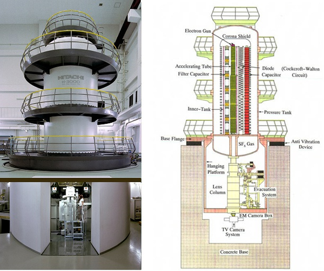
The 3 MV ultra-high voltage electron microscope (Hitachi H-3000) was developed based on various advanced technologies, such as the high stability of the high voltage generating circuit, the reduction of power losses, the improvement of the response of the objective lens, negative ion removal equipment, a remote control system, and an online image processing system. The H-3000 is widely utilized by researchers in many fields, including materials science, nanotechnology, biology, and medical science. The typical advantages of the H-3000 can be summarized as follows:
- Remarkable increases in the maximum observable thickness of specimens
- Various kinds of in-situ observations made possible by the large specimen chamber
- Lattice defect introduction and/or non-equilibrium phase formation through the interaction between high energy electrons and constituent elements in materials.
Main Specifications
1. High Voltage Generator
Symmetrical Cockcroft–Walton circuit: 35-stage
Electricity consumption in high voltage tank: under 1 kW
Acceleration voltage:
Normal: 3.0 MV (3000 kV)
Medium: 0.5, 1.0, 1.5, 2.0, 2.5 MV
Maximum: 3.5 MV
Stability of high voltage: less than 2.0×10⁻⁶/min
2. Electron Gun and Acceleration Tube
Cathode: LaB6 single crystal (thermal type)
Beam current: maximum 20 A
Acceleration tube: 22 kV/step × 138 steps (3 MV)
Insulating gas: SF6 (4 atom)
3. Illumination Lens System
Ion trapping system: electron beam shift
Lens constitution: double-condenser lens
Beam angle: less than 10-3 rad
4. Imaging Lens System
Lens configuration: six-step lens system
(no image rotation)
Magnification: 200 to 1,000,000 (30-step switching)
Camera length at electron diffraction: maximum 14 m
(six-step switching)
Resolution: 0.14 nm
Objective lens
Magnetomotive force: maximum 23 A/V1/2 (3 MV)
Focal length: less than 11 mm
Spherical aberration coefficient: less than 10 mm
Chromatic aberration coefficient: less than 10 nm
Defocused point: minimum 5 nm
5. Specimen Chamber
Holder: Top-entry type and side-entry type
Tilting angle by top-entry type: ±30 degrees
(double tilting)
Tilting angle by side-entry type: ±45 degrees
(double tilting)
Specimen shift: ±1 mm (mechanical system)
±1.5 micro-m (electrical system)
Vacuum: 5×10⁻⁶ Pa (oil-free vacuum system)
6. Camera Chamber
Photo system: imaging plate (32 sheets × 2)
film (50 sheets × 2)
Fluorescent substance: P22, YAG
Fluorescent screen: maximum 60 × 80 mm
Camera system
Digital CMOS camera (2k)
High resolution CCD camera (4k)
Gatan K3 camera
7. Remote Control System
Operation system: Console panel for remote operation
Controlling system: PC and data processing system
Monitoring system: X-ray and oxygen monitors
What is the Materials- and Bio-Science UHVEM ?
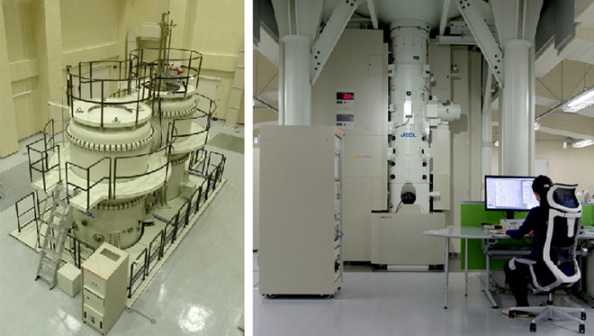
Materials- and bio-science ultra-high voltage electron microscope has the great advantage of high spatial resolution observation of thick specimens up to a few micrometers in thickness due to good permeability of high energy electrons into specimens. Using the merit, it is powerful to researches on nanostructural characterizations of devices, cells, and so on, specially, those on three-dimensional structural analyses in the scale from nanometer to picometer.
Utilizing the additional electron direct detective high speed recording system, in situ observations are possible for materials nano-processes with the time scale of microseconds, and for example, interactions between photon and materials may be investigated in high spatial and time resolution. On the other hand, utilizing the additional stable cryo-stage, biological and soft material specimens are able to be observed under the natural conditions without radiation damages by a combination with the direct electron detection camera.
Main Specifications
1. High Voltage Generator, Electron Gun and Acceleration Tube
Two tanks (Acceleration tube and Cockcroft–Walton circuit)
Cockcroft–Walton circuit
Acceleration tube: 33 steps
Acceleration voltage:
Normal: 1.25, 1.0, 0.8 MV
Maximum: 1.25 MV
High voltage step: 1 kV
Stability of high voltage: less than 8×10⁻⁷/min
Cathode: LaB6 single crystal (thermal type)
Beam current: maximum: 10 μA
Insulating gas: SF6 (0.4 MPa)
2. Imaging Lens System, Resolution and Observation mode
Resolution:
Point resolution: 0.16 nm
Lattice resolution: 0.10 nm
Objective lens
Stability of objective lens: less than 5×10⁻⁷/min
Magnification:
Low magnification mode: x200 ~ 1,500 (9 steps)
Zoom magnification mode: x2,000 ~ 1,200 k (30 steps)
Selected area zoom mode: x20 k ~ 600 (10 steps)
Selected area diffraction mode: less than 10.0 nm・mm (10 steps)
Diffraction mode: λ・L(nm・mm)
3. Cryo-Specimen Chamber
Specimen temperature: less than 100 K
Cryo-transfer system: less than 100 K
4. Image Recording System
CCD camera for monitoring
1 k CCD camera for wide view
2 k CCD camera for image and diffraction recording
4 k direct electron detection camera
5. Electron Energy Spectrometer
Energy Filtering and Energy Spectrum